Labun Nuclear Technologies was established to produce modern, digital electronic parts, boards, and systems that serve as replacements for the analog circuits, instruments, and control systems that were installed in nuclear power plants decades ago. Electronics used in nuclear power plant control rooms and monitoring systems were often developed by manufacturers that no longer offer replacement parts—or available parts no longer fit or cost too much. So when a part or electronic system in a nuclear plant stops functioning, management often asks Doug Labun, owner and president of Labun Nuclear Technologies, to reverse engineer the system in question to develop a modern, digital equivalent.
Labun first began doing this work early in his career while employed at the Vermont Yankee Nuclear Power Plant as an instrumentation and control technician. “I started off replacing components on simple circuits related to converting voltage or reading out radiation levels,” Labun recalls. “When a board malfunctioned because of a bad capacitor, I would simply replace the capacitor. But as time passed, more and more of these types of systems, many of which were installed 30 or 40 years ago, needed to be entirely replaced. It was this demand that led me to establish the business.”
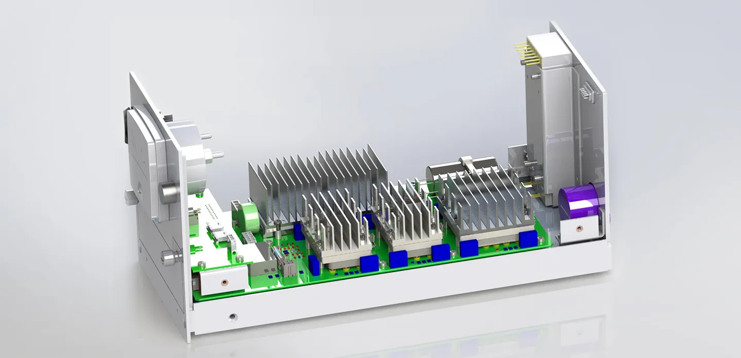
Labun Nuclear Technologies initially reverse engineered replacement boards and systems for nuclear plants using SOLIDWORKS Professional mechanical design software and the PADS® PCB design package. While Labun values the SOLIDWORKS solution for designing system housings and packaging, he believed the lack of integration between the two applications was getting in the way, resulting in time delays and extra costs.
“I had trouble designing boards and getting them out of PADS in a usable format,” Labun recounts. “I realized that what I really needed was a PCB design tool that was compatible with SOLIDWORKS.”
Upon seeing a demo, Labun immediately added SOLIDWORKS PCB powered by Altium PCB design software to its SOLIDWORKS mechanical design installation. Labun Nuclear Technologies chose SOLIDWORKS PCB software because the software is fully integrated with SOLIDWORKS and streamlines board development.
INSTALLED SOLIDWORKS PCB, RELEASED FIRST BOARD NEXT DAY
The day that Labun Nuclear Technologies installed SOLIDWORKS PCB software, Labun began developing an adaptor board for an LCD screen with 40 to 50 components. By the next day, the board was ready for production. “Within the first 48 hours of having SOLIDWORKS PCB software installed, I had my first circuit board design out for manufacturing,” Labun notes.
“From my standpoint, there’s no other combination of tools that can do what SOLIDWORKS and SOLIDWORKS PCB does,” Labun continues. “I can slide back and forth between the two programs without crashes, file conversions, or data transfers. I throw the components on the board in SOLIDWORKS PCB, take the design into SOLIDWORKS to check clearances, move back to SOLIDWORKS PCB to make modifications, and then go back to SOLIDWORKS to automatically generate unified BOM [bill of materials] information and files for production.”