What are Printed Circuit Boards?

Purpose of PCBs
 

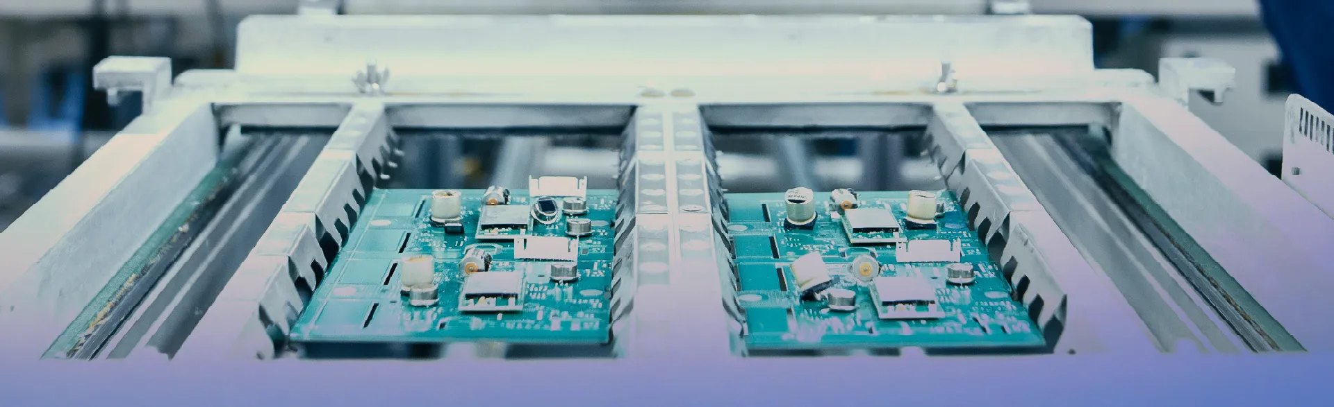
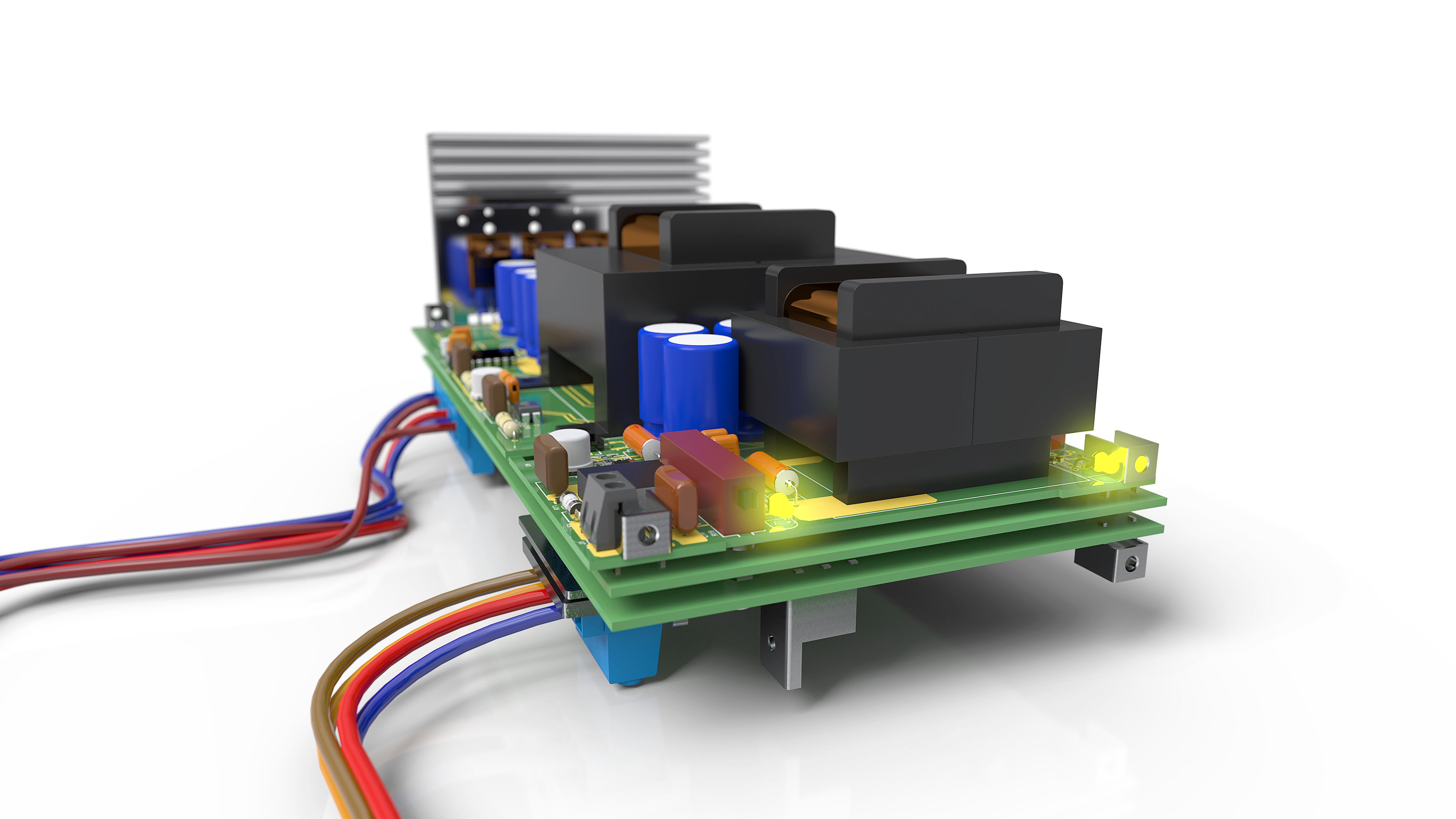
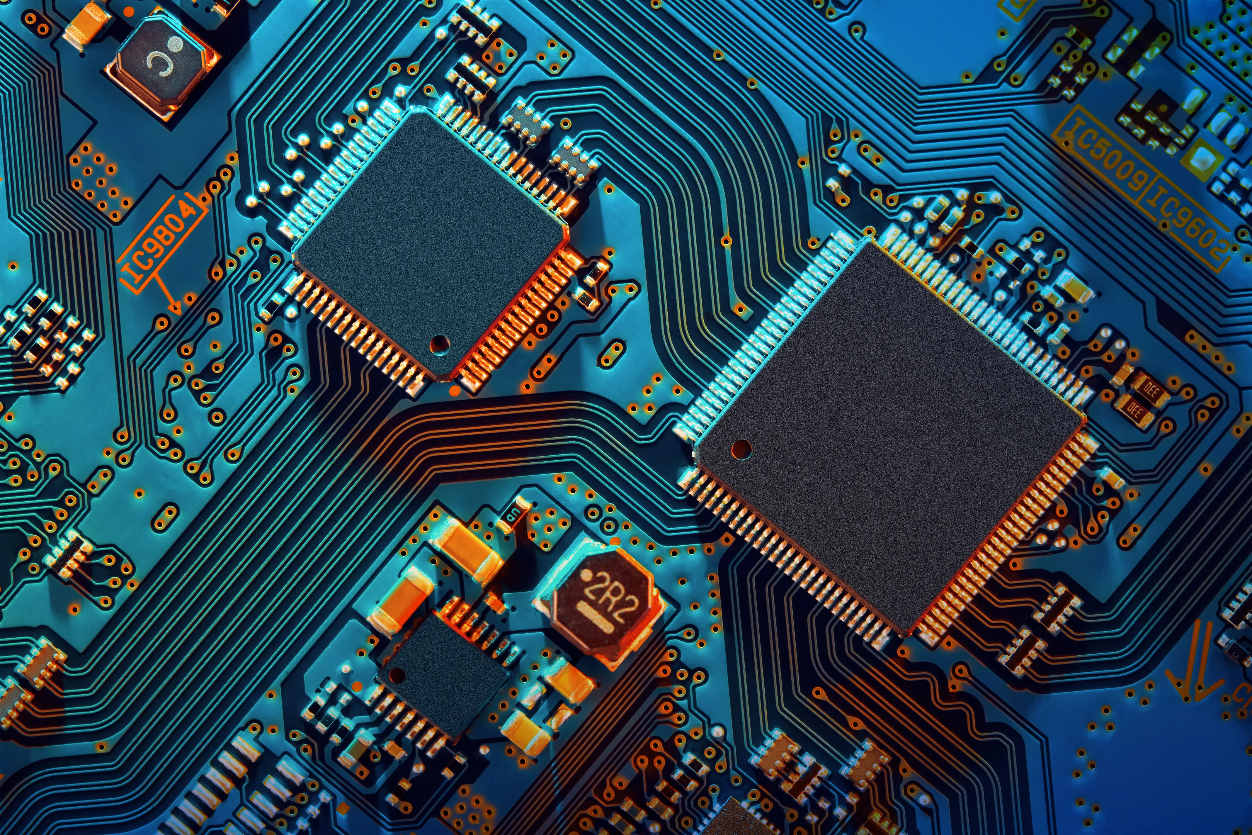
Printed Circuit Boards, or PCBs, are structures that contain and connect electrical circuits. They function as the brain of the system, connecting components to enable different functionalities. You may also hear PCBs referred to as PCAs (printed circuit assemblies) or CCAs (circuit card assemblies).

PCBs are ubiquitous in today’s technology. They represent the general trend in tech to have higher powered systems that take up less physical space. Though ranging in size, PCBs generally demand much less real estate in a product design than other forms of electrical wiring. This space-saving quality of PCBs is one of their main points of appeal in modern product development.

Another key feature of PCBs is their adaptability. Due to the modular nature of their construction, PCBs can be adapted to serve a broad range of functions depending upon your specific use case. Ultimately, PCBs serve the purpose of connecting electronic circuits, thus powering many of the electronic devices we’ve come to depend on today—from smartphones to industrial systems.

How are PCBs Made?

closeup of PCB

Fabrication of PCBs

Comprising of one, two, or multiple layers, PCBs are built via alternating layers of a conductive metal–most always copper–and an insulating layer. The conductive pathways, or traces, are etched, layer by layer, into the copper metal. This is done in one of two ways. The first method has a full copper sheet being laid upon the board. Then, the desired paths for the traces are masked out and a machine is used to etch out the superfluous copper, leaving behind the conductive metal only in the places where the designer intended for there to be traces.

Alternatively, it is possible to leave only the paths of the traces exposed and dip the board into a copper solution. This method coats just the exposed portions of the layer in copper, leaving you with the same end result as the previous method. This second method is sometimes favored if you will be making a lot of PCBs or a many layered PCB as it can be more cost effective since there is less overall copper waste. Regardless of method, this process is repeated until you are left with the desired amount of layers on your board. The completed assembly of all layers of the PCB is often called a “layer stack” or “stackup.”

Interested? Check out CircuitWorks for SOLIDWORKS to learn more about integrating PCBs into your 3D designs View CircuitWorks

Who is Involved in Printed Circuit Board Design?

PCBs are integral electronic components that are necessary for a host of electronic functionalities. Let’s dive in and explore some of the key players involved in PCB design, integration, and production.

PCB Designer avatar

PCB Designer


PCB Designer is a specialized role under the larger umbrella of electronics engineering. The sole focus for a PCB designer is the design and functionality of printed circuit boards. Often requiring knowledge of CAD tools, a PCB designer will own the schematic, component selection, layout, and documentation phases of the design process.

PCB designers need intimate knowledge of the function of the particular board they are designing, and are responsible for making decisions such as the appropriate level of rigidity in the board, the optimal core material, and other material / organizational decisions.

PCB Designer avatar

Electronics Engineer / Systems Architect


Broader than a PCB designer, an electronics engineer or systems architect would be responsible for visualizing the integration of a PCB into the larger electrical system. This could involve things like mapping out connections between PCBs and other inputs, or even determining the optimal arrangement of boards in relation to the system’s requirements.

At a smaller organization, the job functions of a PCB designer and an electronics engineer / systems architect may be collapsed into one role. However, the distinction between the design of the board itself versus the overall mapping and visualization of the overall electrical system is important to make.

Mechanical Engineer


A mechanical engineer will be able to provide a unique perspective into overall part fit, and give guidance on how a part could be changed or a design could be altered to better integrate into the overall product design. Involving a mechanical engineer is paramount when it comes to integrating your PCB into the overall product design.

A mechanical engineer, in addition to the roles above, will have insight into how to best incorporate thermal management into the overall product in order to avoid system overheating, which is a major concern during PCB design and implementation.

PCB Manufacturer


PCB manufacturers are also key players within the PCB design, integration, and production process. Responsible for sourcing the materials required to actually fabricate the PCBs, PCB manufacturers must be looped into conversations throughout the design process as they provide invaluable perspective into what physical resources are available to execute the designs being developed by individuals holding the above titles.

Plus, PCB manufacturing represents a significant portion of the budget for any product containing PCBs, especially for more complex systems. As such, PCB manufacturers represent an important group to involve in conversations surrounding projected costs which is key when presenting a project proposal to management.

Where are Printed Circuit Boards Used?

PCBs are found in almost every modern technological device, ranging from personal smart devices all the way to large industrial systems. Dive into some of these industries below.

Are you a student? Check out these other learning materials. View Learning Content

Our Solutions for Printed Circuit Boards

SOLIDWORKS offers a range of tools to support electrical systems in its SOLIDWORKS Electrical portfolio including those that support the integration of PCBs into CAD designs. Let’s take a look.

CircuitWorks for SOLIDWORKS

screen shot of CircuitWorks

CircuitWorks is an add-in available in SOLIDWORKS CAD software. CircuitWorks brings PCB design into the SOLIDWORKS ecosystem, allowing for further integration between ECAD and MCAD teams. A collaboration tool, CircuitWorks enables users to both import PCB layout information directly to their parametric SOLIDWORKS designs, and define assemblies within SOLIDWORKS that can then be sent to the PCB tool of your choice. This bidirectional design means CircuitWorks works the way you do, augmenting your current workflow

Glossary: Defining Printed Circuit Boards

There’s a lot of unique terminology that comes along with PCBs. Let’s define some of the key terms and concepts related to PCB design, integration, and production.

Term
Definition
Trace

A trace is a conductive pathway, commonly made from copper, that is etched onto its respective layer of the board. Traces can be both internal and external. Internal and external traces differ in their heat dissipation capabilities and other characteristics such as width and thickness. Let’s take a closer look.

Internal Trace
An internal trace is contained within an internal layer of the circuit board. Internal traces have worse heat dissipation as compared to an external trace. As such, care must be taken when selecting the appropriate width, thickness, and routing for these traces to avoid overheating.

External Trace
Conversely, an external trace is found on the top or base of the board. These traces are visible when looking at the assembled board, giving PCBs their characteristic line patterns. External traces are better at thermal regulation than internal traces due to their position on an exposed face of the board.

Hole

A hole in a PCB is any perforation through a board layer. This opening can be made through mechanical drilling, laser removal, or chemical dissolution. There can be structural holes made to secure physical components to the surface of the PCB, or holes to go between layers. The specific shape, size, and orientation of holes in relation to one another are all dependent upon the requirements of the unique board. 

Additionally, PCB holes can be plated or non-plated: 

Plated holes
A plated hole is a hole that has been made and then plated in a conductive metal. These holes are specifically designed to conduct electricity.

Non-plated holes
A non-plated hole is a hole made to go through a layer, or layers, of the PCB that do not conduct electricity. These are generally used for structural purposes rather than to support circuitry as they are not conductive.

Via

A type of plated hole, vias allow for signals to be routed between PCB layers. Key types of vias include:

Through-hole via
A through-hole via runs from the top of the board through to the base, allowing for connectivity through all the layers of the board. These are an effective choice due to their relative ease of manufacturing compared to using a combination of blind and buried vias.

Blind via
A blind via sits either on the top layer or on the base of the PCB. These vias add connectivity between the outside layers of the board and the internal layers. What you then lose in available surface space, you gain in internal layer space.

Buried via
A buried via sits between internal layers carrying signal across either one or multiple internal layers. Converse to a blind via, with buried vias what you lose in internal layer space, you gain in available surface space.

Microvia
A microvia is a specialized via commonly used on HDI (high-density interconnect) PCBs. These vias can be considerably smaller than traditional vias and allow for a higher-density circuit design–letting you fit more functionality in less space.

Keep-In/Keep-Out

Keep-in/keep-out is a phrase you will commonly hear used when discussing PCB design. This relates to the decisions on where, or where not, to design components on the board layer.


Surface Mount Device (SMD) Components

A surface mount device (SMD) component is fastened to the surface of the board via soldering. These components do not run through the board into the internal layers as a through-hole component would. Some common types of SMDs include resistors, inductors, transistors, capacitors, diodes, and integrated controllers (ICs).


Rigidity

Rigidity determines how flexible a board is. There is a range of possible rigidities with the most common forms being described below:

Rigid
A rigid PCB is inflexible. Still the most common type of PCB, rigid boards are ideal for low-stress environments and standard geometries. Rigid boards are also comparatively simple to manufacture as compared to other rigidities and are ideal for mass production as well.

Flex
A flex PCB is a completely flexible circuit. Flex PCBs are commonly made on polyimide–essentially a highly flexible, heat resistant plastic. Flex PCBs are ideal for irregular geometries due to their flexibility, and are commonly found in devices like personal wearables.

Rigid-Flex
A rigid-flex PCB combines elements of both rigid and flex PCBs. These boards are ideal thanks to their ability to absorb a higher threshold of mechanical shock as compared to a rigid board, and their unique combination of flexibility and durability due to the combination of rigid and flex elements. While they may require more design considerations compared to other board types for things like bend radius and mechanical strain, once these boards are constructed they are excellent options for custom designs and any range of product use cases–from personal to industrial.

Prepregs

Prepreg, from “pre-impregnated,” is an insulating layer on a multilayer PCB. Generally made from resin-impregnated fiberglass, prepreg layers are essential for connecting and insulating the copper layers of the PCB. Separate prepreg layers—outside of their use in core assembly—are generally not needed on a single layer board since there is only one conductive layer on a single layer board and thus no need for the additional layer separation provided by prepregs.


Cores

A core in a PCB is sometimes also referred to as the base of the PCB or as the board substrate. The cores are pre-pressed layers. The core or substrate material is sandwiched between layers of copper foil and prepreg materials respectively. Cores are commonly made of a fiberglass-resin mix similar to prepregs as described above which you may see written as “FR4” cores/PCBs. Cores may also be made or enhanced with ceramics for improved thermal conductivity, or may alternatively be made of metal for use in a metal-core PCB which has additional structural benefits. Your choice of core will depend upon your desired use case and the environment in which your board will be deployed.


Silkscreen

A silkscreen is the topmost layer of the PCB. This is one of the last steps in the manufacturing process. Usually done in white, the silkscreen layer is used for labelling, branding, and any other written information needed on the board.


Solder Mask

Sometimes also referred to as a solder resist, a solder mask covers the full PCB leaving out the areas where soldering needs to occur. Usually green in color, though possibly red or black, solder masks help prevent shorts by physically and electrically insulating traces on the board.


Gerber Files

A gerber file is a common manufacturing file type that is the standard way of communicating board specifications with a manufacturer.


ODB++ Files

ODB++ files are another way to communicate between design and manufacturing. They are an effective way to communicate PCB design information between CAD and CAM tools, and thus between design/engineering and manufacturing teams.